
Double Exposure Lithography
The current optical photolithography technology is approaching the physical barrier to the minimum achievable feature size. To produce smaller devices, new resolution enhancement technologies must be developed. Double exposure lithography has shown promise as potential pathway that is attractive because it is much cheaper than double patterning lithography and it can be deployed on existing imaging tools.
Double Exposure Lithography versus Double Patterning Lithography
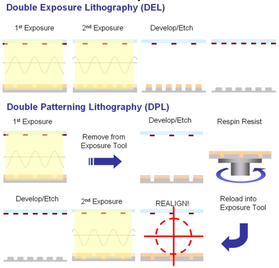
Double exposure lithography (DEL) and double patterning lithography (DPL) are proposed approaches to performing the two exposure passes. DEL is defined as a two exposure pass lithographic process that does not require the removal of the wafer from the exposure tool chuck between passes. DPL is defined as a two exposure pass lithographic process that requires a chemical development of the photoresist layers and possibly an intermediate etch step. The DPL processing approaches will require the removal of the wafer from the exposure tool chuck and loss of overlay registration. DEL and DPL processes are illustrated in Figure 1.
The benefits of DEL and DPL principally include the ability to use existing exposure tools to print technology nodes below the NA limit for single exposure processes. This could mean a lower cost of ownership as these techniques can in principle be deployed without costly capital investment. However, the two exposure passes require doubling the number of masks and reduced throughput due to increased processing time. The process time is dramatically increased in the DPL process because of the additional process steps compared to the DEL process. In addition, the removal of the wafer from the wafer chuck between exposures poses severe overlay issues that may be difficult to overcome, especially at the CDs where this technology will be implemented. The DEL process only introduces an additional exposure pass, and since the wafer is not removed from the imaging tool between exposures, the overlay issues are minimized. The reduced cost of ownership of DEL suggests that it would be the preferred technique. However, this technology is not possible without the development of new materials with nonlinear response to exposure dose.
The goal of this project is to develop identify materials that have nonlinear response to exposure dose and develop systems that will operate within the current manufacturing framework.
Continue Reading >> Resist Memory