|
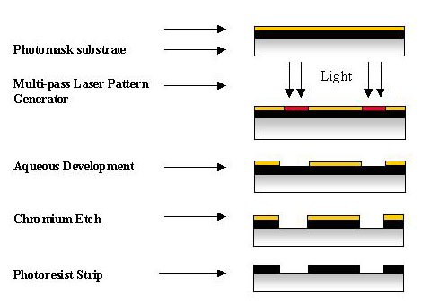
The photoresist process
used in photomask fabrication involves process steps
that are similar to photoresist processes used to make
silicon devices. The mask blank is a 6 in. x 6 in.
quartz blank with a thickness of 0.25 in. The blank is
coated with a film stack that is a non-homogeneous
layer of chromium oxide (200 Å) on top of a thin
layer of pure chromium (800 Å). The chromium layer
provides an opaque and mechanically strong layer to
prevent light penetration through the mask. The
chromium oxide layer is grown on the chromium layer to
minimize the reflections off of the mask.
The photomask is coated with photoresist and then
baked (post-application) to remove solvent from the
resist. A laser pattern generator is then used to
expose the individual features of the circuit pattern
on the resist-coated mask. The exposure time takes
hours, which is the rate limiting step in the
photomask fabrication process.
The exposed photoresist is then developed with an
aqueous base developer (commonly tetramethyl ammonium
hydroxide-TMAH). The features are then etched into the
chromium layer and the remaining photoresist is
stripped off the photomask to complete the pattern
transfer process into the chromium layer.
|