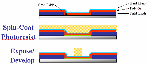
Patterning Over Topography |
| In modern production processes, it is imperative that a patterning
technique facilitate patterning over existing topography, since the
substrates commonly posses at least marginal and sometimes extreme
topography. Projection lithography has the ability to expose patterns
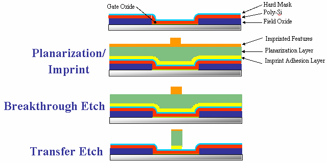
among topography, as shown in Figure 1. SFIL requires a planar
substrate on which to imprint, and so an imprint planarization step is
added to the SFIL process flow, as shown in Figure 2. |
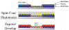 |
| Figure 1. Schematic of conventional resist processing. |
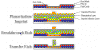 |
| Figure 2. SFIL process flow with the addition of an
imprint planarization layer. |
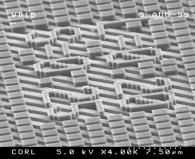
| In a collaborative effort with
Agilent Technologies, PMMA (497,000 MW) was spun at 6000 RPM to
provide a thin organic layer over a pre-patterned substrate, typically a
grating structure. Then, a planarization layer of an acrylate
photopolymer was cured over the hard-baked PMMA using a non-patterned
optical flat for the imprint template. Finally, the etch barrier was
patterned over the planarized organic layer. High aspect ratio resist
features such as those shown in Figure 3 were generated using the same
etch transfer process as that used for flat
substrates.
|
a) b)
b) c)
c) |
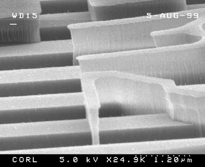
| Figure 3. Examples of polymer features on extreme
topography. The underlying line'space array is a 700 nm tall Fresnel
lens in Si. |

 b)
b)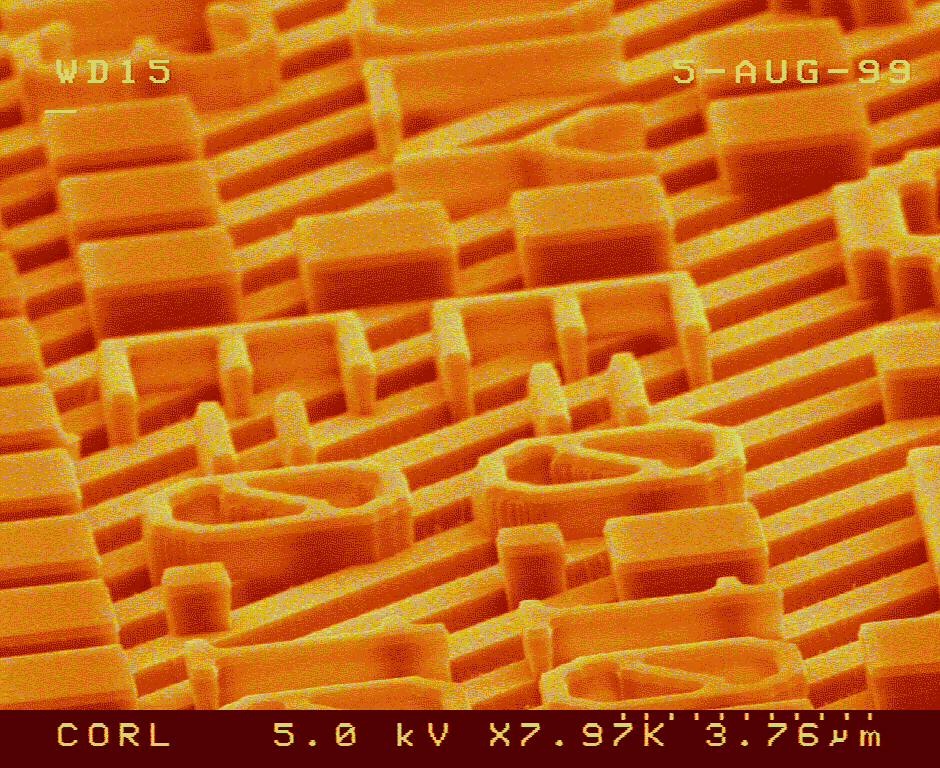 c)
c)