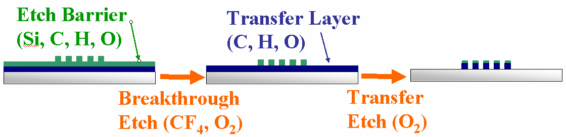
Etch Transfer |
| The SFIL process flow
depicts etching steps which allow amplification of the imprinted feature
aspect ratio by etching into a polymer underlayer. The etch barrier
contains Si, C, O, and H, while the transfer layer contains C, O, and H.
The existence of the Si in the etch barrier provides the etch resistance
needed to etch into the transfer layer with O2 RIE, but also
requires fluorocarbon etch chemistries in order to break through the
residual imprint layer. This is shown pictorially in Figure 1. |
 |
| Figure 1. Schematic diagram of post-imprint etch
processing. |
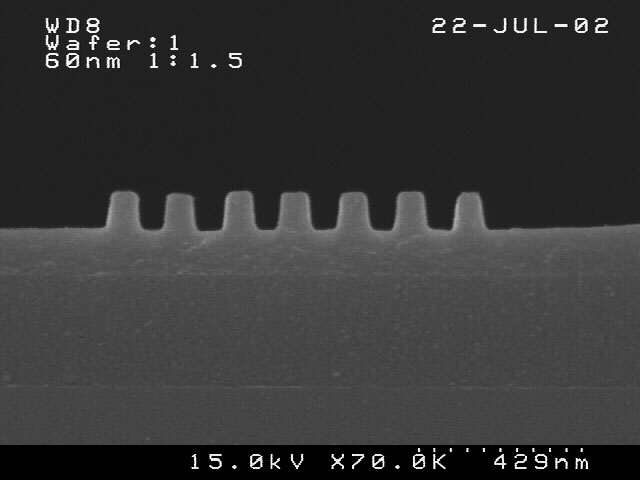
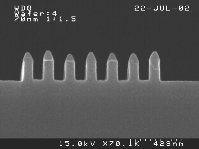
| As a demonstration of the etch process, a sample wafer was processes using
CHF3/O2 breakthrough etch, and O2
transfer etch, as described in
Johnson (2003), and the results are shown in
Figure 2. The imprinted features (Figure 2a) show fairly square
feature profiles, while some faceting is observed throughout the
breakthrough etch (Figures 2b and c). This faceting results from the
anisotropic etch conditions, and is observed in conventional resist
processing as well, as shown in Figure 3. |
a) b)
b) c)
c) |
d)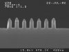 e)
e)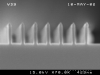 |
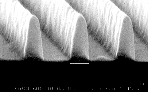
| Figure 2. Etch transfer in action.
a) Imprinted image with ~150 nm residual layer, b) part-way through
breakthrough etch, c) after completion of breakthrough etch, d) part-way
through transfer wtch, and e) after completion of the transfer etch.
These are not from the same L/S array, since the samples had to be
destroyed for SEM analysis. Figure 3e shows 40 nm lines approximately
400 nm tall. |
a)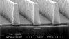 b)
b)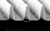 |
| Figure 3. KrF resist images a) before and b) after ARC
etch, showing the appearance of feature faceting arising from the
anisotropic etch conditions. |

 b)
b) c)
c)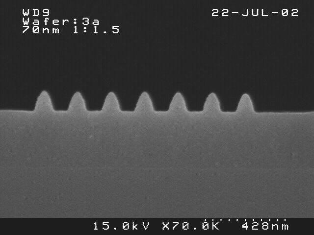
 e)
e)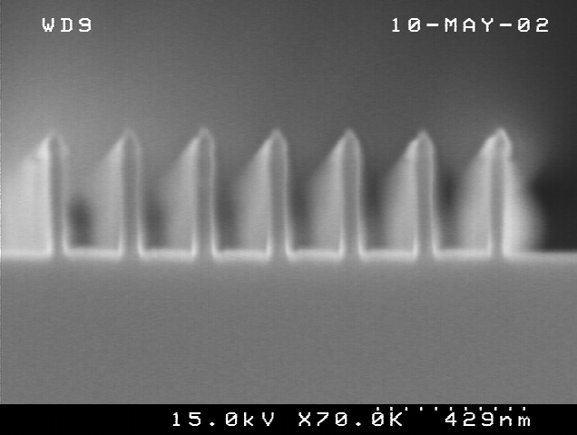
 b)
b)