 |
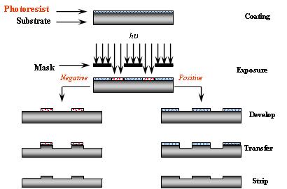
| Figure 1 |
Background |
| The resolution (R) of the lithographic process is defined by the Rayleigh
Equation, |
| where k1 is known as the Rayleigh coefficient,
l
is the vacuum wavelength of the exposing radiation, n is the index of
refraction of the ambient medium through which the exposing radiation is
focused,q
is the angular half aperture of the lens and NA stands for the numerical
aperture of the lens. [2] |
| Improvements in lithographic patterning have led to the continual
shrinking of device feature sizes and the resulting performance
improvements and cost reductions seen in todays electronic devices.
These improvements have historically been achieved through the
development of new exposure sources with lower wavelengths.
Accompanying incremental improvements in the lens system by the
reduction of k1 and the increase of NA through larger qs
have also contributed. |
| Early exposure tools used 436 nm light from the
g-line emission of a mercury arc lamp, followed by 365 nm light from its
i-line emission. Krypton-fluorine (KrF) excimer lasers then replaced
mercury arc lamps for leading edge lithography with 248 nm light, and
the state of the art is now argon-fluorine (ArF) lasers producing light
at 193 nm. |
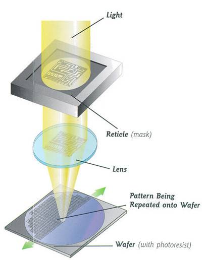
|
| Illustration of exposure through mask and focusing by lens.
|
| With each step down in wavelength, optical systems had to be redesigned and new
materials have had to be developed.[3] To move below 193 nm, the
development is complicated by the need for completely new materials for
the lens systems as well as the photoresist platforms and the necessity
for exposure to take place in vacuum. The rising costs of such
development has led to the resurrection of a novel lithographic process
first proposed in the 1980s called immersion lithography.[4][5][6][7]
Immersion lithography with the 193 nm exposure wavelength is now
considered the most likely candidate for printing features at 45nm and
below.[8] |
| Continue to Immersion Lithography Theory |
References |
| 1. Thompson, L.F.; Willson, C.G.; Bowden, M.J. Introduction to Microlithography.
American Chemical Society, Washington, DC. 1989.
|
| 2. M. Switkes, M. Rothschild, R. R. Kunz, S-Y. Baek, D. Cole, M. Yeung,
Microlithography World 12(2), 4, 2003.
|
| 3. Stewart, M.D.; Patterson, K.; Somervell, M.H.; Willson, C.G. J.
Phys. Org. Chem. 2000; 13: 767-774.
|
| 4. A. Takanashi et al., US Patent No. 4480910,
6 Nov. 1984
|
| 5. Lin, B. J. Microelectron. Eng.1987,
6, 31.
|
| 6. Kawata, J.; Carter, J. M.; Yen, A.; Smith, H. I. Microelectron.
Eng. 1989, 9, 31.
|
| 7. H. Kawata, I. Matsumura, H. Yoshida, K. Murata, Jpn. J. Appl.
Phys. 31, 4174, 1992.
|
| 8. International Technology Roadmap for Semiconductors: http://public.itrs.net/
|
Version History |
| Original page created 02/23/06 |
| | |