SFIL Templates |
| (Much of this work was carried out by
Motorola Labs.1-4) |
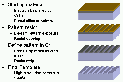
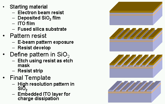
| SFIL imprint templates are fabricated using an analog of
the photomask fabrication process. In a typical Cr-based template
process, a 6-in ´ 6-in ´
¼-in fused silica reticle blank coated with a thin Cr film is
spin-coated with an electron beam resist, and baked to drive off excess
casting solvent. The plate is then exposed in a high resolution
direct-write e-beam tool. The resist is then developed, leaving a resist
pattern that exposes selected portions of the underlying Cr film. This
resist pattern is used as an etch mask to pattern the Cr with Cl-based
RIE. The resist is removed after etching, leaving behind a patterned Cr
layer on the silica substrate. A fluorine-based RIE transfers the image
into the fused silica substrate to a depth of 100 to 200 nm, depending
on design constraints. The Cr layer is typically left on the templates
until after the cutting process, which is described below; this
facilitates template pattern recognition, and minimizes mistakes in
cutting. |
 |
| Figure 1. Standard Cr-based SFIL template fabrication
process. |
| The Cr layer is not used
in the SFIL process as a photon absorber as it is in projection
lithography, but it serves only as a charge dissipation layer during
e-beam patterning and as a hard mask during the quartz feature
definition etch. As a result, the Cr layer needs to be only thick enough
to possess a sufficient conductivity and to withstand the SiO2
etching. The template fabrication process was modified to by thinning
the Cr layer from ~1000 Å to ~100 Å, and also by using a thinner layer
of e-beam resist. These process modifications have provided the ability
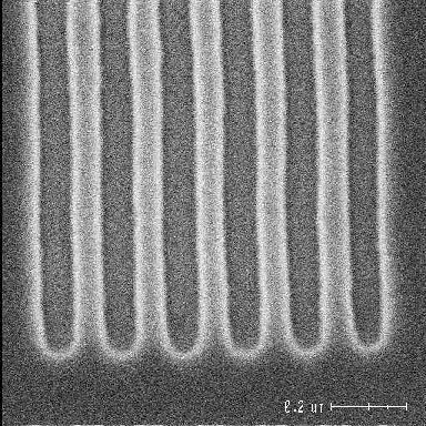
to fabricate templates with features smaller than 20 nm. Figure 2 shows
SEM images of template features down to 20 nm. |
a)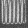 b)
b) 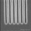 c)
c)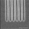 d)
d)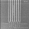 |
| Figure 2. SEM images of templates fabricated using the
thin-Cr process. a) 60 nm, b) 40 nm, c) 30 nm, and d) 20 nm features. |
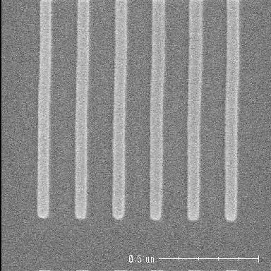
| Template fabrication schemes employing a transparent
conducting oxide into the final template have also been investigated.
The addition of a blanket conducting layer dissipates charge during SEM
inspection of the final templates. One such scheme involves coating the
fused silica plate with a film of indium tin oxide (ITO), which is
transparent and conducting. The ITO film is then covered with a film of
deposited SiO2, followed by e-beam resist. The resist is
patterned using an e-beam tool, and chemically developed. The patterned
resist is used as an etch mask to pattern the underlying SiO2
film. A convenient result is that the ITO serves as an etch stop for the
SiO2 etch process. The resist is finally stripped, resulting
in an imprint template of patterned SiO2 features resting on
a blanket film of ITO on fused silica substrate. The SiO2
features will define the imprinted features in the SFIL process, while
the ITO film is transparent to allow the SFIL process exposure and
conducting to allow SEM inspection of the template. |
 |
| Figure 3. ITO-based SFIL template fabrication process. |
| An added benefit of this process is that since the ITO
serves as an etch stop for the SiO2 patterning etch, the
template feature depth is defined solely by the thickness of the
deposited SiO2 film. SEM images of templates made using this
process are shown in Figure 4. |
 |
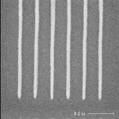
| Figure 4. SEM image of 20 nm template feature fabricated
using the ITO process. |
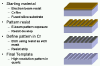
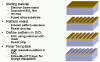
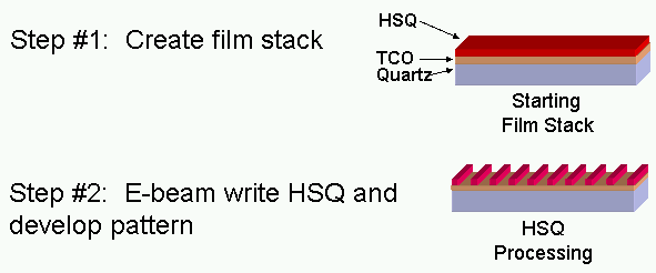
| A third template fabrication scheme
consists of spinning a film of hydrogen silsesquioxane (HSQ) on the ITO
layer, as shown in Figure 5. The HSQ is directly written with e-beam
lithography, and the unexposed regions are developed away, leaving the
cured HSQ topography. In its cured state, HSQ becomes a durable oxide
making it a very convenient material for direct patterning of SFIL
template relief structures. One benefit of this scheme is that it
eliminates the etching processes associated with other template
fabrication methods. |
 |
| Figure 5. HSQ-based SFIL template fabrication process. |
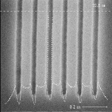
| This process is by nature a negative-tone process. Figure
6 shows SEMs of an HSQ template demonstrating resolution as small as 20
nm. |
a)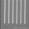 b)
b)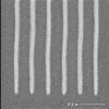 c)
c)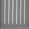 |
| Figure 6. SEM images of HSQ-based template. a) 60 nm, b)
20 nm features. |
-
D.J. Resnick, et al..
"High Resolution Templates for Step and Flash Imprint Lithography."
Proc. SPIE 4688: 205 (2002).
-
W.J. Dauksher, et al..
"Characterization of and Imprint Results using ITO-based Step and Flash
Imprint Lithography Templates." J. Vac. Sci. Tech. B 20(6):
2857-2861 (2002).
-
D.P. Mancini, et al.. "Hydrogen Silsesquioxane for Direct E-beam
Patterning of Step and Flash Imprint Lithography Templates." J. Vac.
Sci. Tech. B 20(6): 2896-2901 (2002).
-
T.C. Bailey, et al.. "Template Fabrication Schemes
for Step and Flash Imprint Lithography." Microelectron. Eng.
61-62: 461 (2001).
|

 b)
b)  c)
c)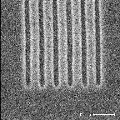 d)
d)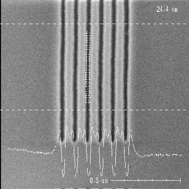
 b)
b)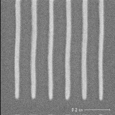 c)
c)