|
||||||||||
|
Overlay Alignment Figure 1 compares the overlay mark configurations for optical projection step and scan lithography and for the SFIL process. In optical step-and-scan lithography tools, alignment is performed i) to align the mask relative to the mask stage, ii) to align the wafer relative to the wafer stage, and iii) to align the mask and the wafer relative to each other using multiple reference mirrors. Calibration of these step and scan tools essentially involves proper alignment of all of these reference mirrors with respect to the mask and wafer stages. In order to maintain the calibration, the tool must be carefully monitored for thermal, vibrational and mechanical contributions to pattern distortions. The SFIL process has the advantage of not requiring mirror and/or calibration of this sort.
Figure 1. Overlay mark configuration for projection step-and-scan and SFIL. Overlay marks and the overlay error measurements can be readily developed for SFIL by adapting existing techniques. It is expected that the overlay measurement techniques developed and demonstrated for X-ray proximity printing can be adapted to SFIL. When the gap between the template and wafer is small, two layers of overlay patterns, such as box-in-box or cross-in-box, can be simultaneously acquired without difficulty using conventional microscopes. In a simple experiment, a Vernier pattern such as in Figure 2 was imprinted on a wafer, and the same pattern was imprinted on the existing pattern. The goal was to align the second pattern on the first, to determine if the SFIL materials and template provided sufficient image contrast for alignment. Using this technique, an estimate of the overlay error can be obtained by identifying the darkest block of grating lines that have equal line and space widths.
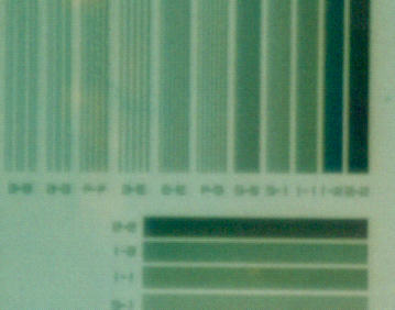
Figure 2. Schematic of Vernier pattern used for preliminary overlay alignment experiment. When the patterns are overlaid, the overlay error is equal to the line width of the grating pattern in the darkest block. If multiple blocks have the same level of darkness, the block that has the largest lines/spaces specifies the error. While more sophisticated techniques, such as the Moiré fringe method, can significantly improve the overlay measurement resolution, we did not pursue them at this time because our stage is limited to a resolution of about 0.5 mm. Figure 3 is an optical micrograph through the template of a mis-aligned pattern. Note that the existing image is clearly visible through the template and liquid etch barrier layer.
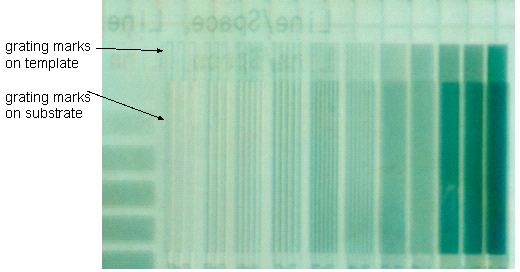
Figure 3. Optical micrograph through template during alignment feasibility test demonstrating the ability to resolve both the template pattern and the substrate pattern. The wafer was aligned to within the capabilities of the modified mask aligner, and the resulting micrographs are shown in Figure 4. An imprint that includes two well-aligned layers is shown in Figure 4. At the resolution limit of the current alignment stage, only the block of 0.5/0.5 mm grating becomes the dark as shown in Figure 4, which indicates that overlay of alignment accuracy of 0.5 mm has been achieved both in X and Y directions simultaneously.
Figure 4. Optical micrographs of grating marks showing alignment accuracy of 0.5 mm in X and Y. | ||||||||||
|
|
||||||||||