|
||||||||||
|
MOSFET Device SFIL was used to pattern the poly-Si gate in a MOSFET device. Figure 1(a) shows a simplified industrial MOSFET process flow for the fabrication of the transistor gate. In this process, the starting substrate is a wafer in which the field oxide and the gate oxide has been grown, the poly-Si deposited, and the oxide hard mask in place, This would be spin-coated with resist, exposed, and developed leaving the patterned resist features. These resist features would then serve as an etch mask to pattern the hard mask and ultimately pattern the underlying poly-Si for the transistor gate. The SFIL technique replaces the spin-coating and exposing steps used in conventional lithography with the process flow seen in Figure 1(b) and described below.
Figure 1. (a) Simplified industry MOSFET process flow for gate fabrication. (b) Additional steps employed by SFIL. The starting substrate was a Si wafer that possessed gate oxide, isolating field oxide, and blanket poly-Si and hardmask films. A layer of poly(hydroxystyrene) was spin-coated to act as an adhesion layer for the imprint planarization step. Imprint planarization was performed using 4% Darocur 1173 (Ciba) in ethylene glycol diacrylate and imprinting with a blank template. The standard SFIL process was performed on this substrate. The alignment was performed on an existing Canon 501 mask aligner at that has been modified for the SFIL process. Using optical microscopy, this tool has the capability of detecting alignment error, making the corresponding corrections in X, Y, and theta, and performing the UV exposure to complete the imprint. The process was performed by first manually dispensing a small amount of etch barrier on the wafer in the area to be imprinted. The wafer was then raised on a hydraulic piston into close proximity of the template. As the etch barrier filled the template relief patterns, a thin layer of fluid prevents the wafer from actually making contact with template. This thin fluid film, referred to as the residual layer, acts as both a lubricant and a damping agent allowing adjustment in the alignment to be made. With a small gap of ~0.25 mm between the template and the wafer, both the alignment marks on the wafer surface and the template are in focus through the backside of the template and fine alignment could be performed with minimal optical errors. Alignment between the underlying poly-Si and the SFIL patterned template was required to define the gate structures over the active areas of the wafer. Rough alignment in the theta direction was performed using a simple cross-in-box pattern. The cross feature was previously defined on the wafer surface and the box pattern was present in the relief image on the template. Fine alignment was performed using Vernier marks in the X and Y directions. The alignment resolution could be resolved from the resulting imprint by determining which marks on the Vernier scale were aligned. With the center marks aligned, the resulting overlay error was found to be less than 0.25 mm. Following the iterative process of alignment, the imprint area was irradiated with UV light, polymerizing the etch barrier and leaving an organosilicon relief image that is a replica of the template pattern, an example of which is shown in Figure 2.
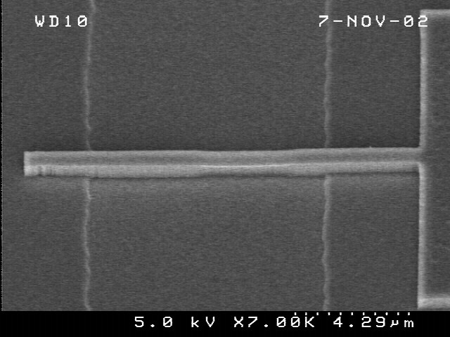
Figure 2. Example polymer gate structure. The standard etch sequence was performed to etch through the residual layer, transfer layer, hardmask, and poly-Si. The remaining fabrication steps were completed using conventional processing techniques. Following gate patterning, each wafer underwent implantation, isolation oxide growth, contact patterning, and aluminum deposition. An example of one of the completed devices used in these experiments is shown in Figure 3 . These devices did not undergo an anti-punch-through implant, source/drain extensions, or silicide gate cap due to time constraints on the project. These steps are within our processing capability and will be included in future device fabrication processes.
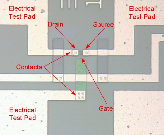
Figure 3. Completed MOSFET device. Following processing, the completed devices were electrically tested. Both drain current vs. drain voltage (Id vs. Vd) and drain current vs. gate voltage (Id vs. Vg) curves were obtained and can be seen in Figure 4. These I-V curves confirm the functionality of the fabricated MOSFET devices and the successful incorporation of SFIL in creating a working electrical device. The electrical data are also consistent with other electrical devices fabricated with conventional lithographic techniques using similar processing equipment
a) Figure 4. (a) Ig vs. Vg curves for sintered PMOSFET, Ltarget = 2 mm, W = 23 mm. (b) Id vs. Vd curves for sintered PMOSFET, Ltarget = 2 mm, W = 23 mm.
| ||||||||||
|
|
||||||||||