|
||||||||||
|
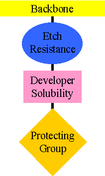
Development of 157 Photoresist Materials The purpose of this document is to provide timely public access to the 157 nm resist development work being done in our laboratories under contract from International SEMATECH. It is our goal and SEMATECH's goal to disseminate this information as rapidly and widely as possible in hope that doing so will accelerate the availability of 157 nm resist materials to the members of International SEMATECH. 157 nm Photoresist Project Introduction Within the last several years, the extension of optical lithography from 193 nm to 157 nm has garnered widespread support as it offers the prospect of continued resolution improvement based on expertise acquired over decades of implementing these optical methods. However, the development of new photoresist materials must take place within an extremely compressed time frame. If one considers that development of 248 nm materials took approximately 10 years, and more recently the development of 193 nm has taken place within the span of 8 years, the developers of 157 nm photoresist materials face a highly compressed research schedule. Modular approach to 157 nm photoresist polymer design In developing materials for 193 nm photoresists, potential polymers were considered as a single entity that offered all of the necessary characteristics for the final photoresist including etch resistance, ability to modify its solubility characteristics in the exposed regions, and transparency at the exposure wavelength. This type of approach requires that polymer design candidates be developed to a sufficient level of maturity in order to allow for a fair comparison among them. Due to the abbreviated development schedule for 157 nm photoresists, our research group has chosen to abandon this approach and adopt more of a “divide and conquer” system for identifying and constructing promising polymer designs. The total photoresist design has been broken down into four functional modules, each of which is responsible for imparting one necessary characteristic into the final polymer. This allows for each subunit to be addressed in a somewhat independent fashion rather than considering the whole design simultaneously. It is critical to remember that transparency requirements must be considered in the development of every subgroup. Our model breaks the total photoresist polymer design into four modules: backbone, etch barrier, acid group, and protecting group. Modular approaches have been taken in the development of photoresist designs in the past. For instance, in the IBM version 2 193 nm photoresist, a separate monomer is added to the polymer to impart each of the necessary requirements (1). In the present case, the monomers themselves are being designed in a modular fashion.
Document Structures The remainder of this document details our progress on this project. The following pages will be frequently updated to describe new findings. 1) Allen, R. D., Wallraff, G. M., Hofer, D. C., Kunz, R. R. IBM J. Res. Develop. 1997, 41, 95. Version History Original page created 03/18/99 New page created 05/02/00 Update 1 05/03/00 Update 2 05/15/00 | |||||||||
|
|
||||||||||