|
|
||
|
Top Surface Imaging (Best
viewed thru Internet Explorer)
The top surface imaging
process being studied in this project is a modification of the chemical
amplification scheme. It
utilizes the same coating and exposure technology, but the steps that
follow are much different than those used in traditional lithography
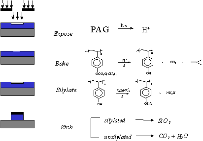
processes, as shown below (with TBOC-Styrene as an example).
Figure 1: Silylation Lithographic Scheme After the traditional exposure
and bake processes, the next step is to silylate the photoresist.
The resist is placed in a silylation chamber where it is exposed
to the vapor of a reactive, silicon containing agent.
The alcohol groups in the exposed regions of the resist can react
with the silylating agent while the TBOC groups in the unexposed region
cannot. The silylation of
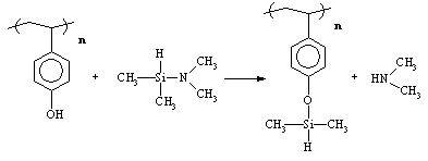
the phenolic functionality is shown below in the poly(hydroxystyrene)
system, using dimethylsilyldimethylamine (DMSDMA):
The result of the silylation
reaction is to incorporate silicon atoms exclusively into the exposed
region of the photoresist. Many
different polymer structures and silylation agents may be used.
The next step is to place the wafer
into an oxygen plasma tool (reactive ion etcher) to develop the images.
In the presence of an oxygen plasma, the silicon-containing
regions oxidize to form a thin layer of SiO2 at the top of
the resist. The SiO2
acts as an etch barrier and protects the underlying photoresist and
substrate. In the regions
where there has been no silicon atom incorporation, the oxygen plasma
completely oxidizes the resist to carbon dioxide and water, which are
pumped from the system.
Background on Thin Layer
Imaging (click
here for more details) | |
|
|
||


