
Synthesis and practical applications of two cutting edge nanomaterials
The ability to reliably synthesize large amounts of high quality nanomaterials remains a formidable barrier to their utilization in next-generation technologies. We are investigated unique ways to produce large amounts of both graphene and boron nitride nanotubes, as well as looking into non-canonical applications of them in the semiconductor industry.
Graphene
Polymer-based transfer of graphene
Graphene, a substance 200 times stronger than steel yet only a single atom thick, has only recently been discovered in the lab. Spurred on by a perhaps optimistic Nobel Prize, graphene has ignited a global scientific gold rush, as companies and universities racing to understand, patent and profit from this glamorous cousin of ordinary pencil lead. Currently, chemical vapor deposition on transitional metal surface is able to yield high-quality graphene at a large scale. (ref. http://www.sciencemag.org/content/342/6159/720.abstract) However, how to transfer the atomic-thick carbon film from metal surface to target substrate remains a major challenge for this community.1. Selection of polymer support
Polymethyl methacrylate (PMMA) is the material overwhelmingly used during graphene transfer- the polymer support is removed by a chemical or thermal treatment to yield graphene sheets. However, the resulting PMMA residues on graphene limit its performance. By studying kinetics of polymer dissolution and developing methods to visualize these surface residues, we are able to show molecular-scale pictures of this process and accordingly reduce the surface contamination with proper polymer specifications. New polymer which will release a clean surface (such as self-immolative polymers) will also be synthesized and tested.2. Graphene delamination from metal surface
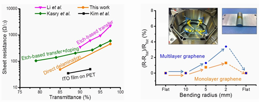
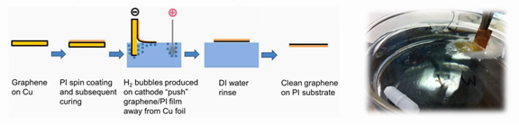 Instead of standard copper etching, we developed electrochemical delamination to detach graphene film from metal surface. In this process, the copper substrate can be preserved after transfer and reused for graphene growth. Moreover, we found electrochemical delamination results in a clean graphene surface and therefore good electrical properties, promising for flexible electronics. (ref. http://onlinelibrary.wiley.com/doi/10.1002/smll.201301892/abstract)
 We are also working on mechanical peeling method. By engineering the graphene-polymer interaction, we will obtain a continuous graphene film while simultaneously modify its electrical properties as needed.